- 您现在的位置:买卖IC网 > Sheet目录322 > DS2433X-S#T (Maxim Integrated)IC EEPROM 4KBIT 6FCHIP
�� ����
����
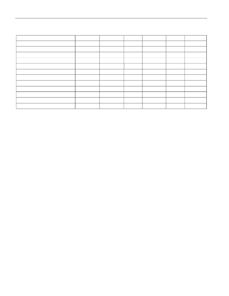
����DS2433�
�AC� ELECTRICAL� CHARACTERISTICS—OVERDRIVE� SPEED�
�(� T� A� =� -40� ?� C� to� +85� ?� C.� )�
�PARAMETER�
�Time� Slot�
�Write� 1� Low� Time�
�Write� 0� Low� Time�
�Read� Low� Time�
�Read� Data� Valid�
�Release� Time�
�Read� Data� Setup�
�SYMBOL�
�t� SLOT�
�t� LOW1�
�t� LOW0�
�t� LOWR�
�t� RDV�
�t� RELEASE�
�t� SU�
�MIN�
�6�
�1�
�6�
�1�
�0�
�TYP�
�2�
�1.5�
�MAX�
�16�
�2�
�16�
�2�
�4�
�1�
�UNITS�
�?� s�
�?� s�
�?� s�
�?� s�
�?� s�
�?� s�
�?� s�
�NOTES�
�8�
�8�
�9�
�10�
�Recovery� Time�
�t� REC�
�1�
�?� s�
�Reset� Time� High�
�t� RSTH�
�48�
�?� s�
�11�
�Reset� Time� Low�
�Presence� Detect� High�
�Presence� Detect� Low�
�t� RSTL�
�t� PDHIGH�
�t� PDLOW�
�48�
�2�
�8�
�80�
�6�
�24�
�?� s�
�?� s�
�?� s�
�NOTES:�
�1)�
�2)�
�3)�
�4)�
�5)�
�V� PUP� =� external� pullup� voltage.� See� Figure� 8.�
�All� voltages� are� referenced� to� ground.�
�V� IH� is� a� function� of� the� external� pullup� resistor� and� V� PUP� .�
�Input� load� is� to� ground.�
�The� Copy� Scratchpad� takes� 5ms� maximum� during� which� the� voltage� on� the� 1-Wire� bus� must� not� fall�
�below� 2.8V.�
�6)� Capacitance� on� the� data� pin� could� be� 800pF� when� power� is� first� applied.� If� a� 5k� ??� resistor� is� used� to�
�pull� up� the� data� line� to� V� PUP� ,� 5� ?� s� after� power� has� been� applied� the� parasite� capacitance� will� not� affect�
�normal� communications.�
�7)� During� the� execution� of� the� Copy� Scratchpad� command� the� DS2433� automatically� erases� the� memory�
�locations� to� be� written� to.� No� extra� steps� need� to� be� taken� by� the� bus� master.�
�8)� The� duration� of� the� low� pulse� sent� by� the� master� should� be� a� minimum� of� 1� μ� s� with� a� maximum� value�
�as� short� as� possible� to� allow� time� for� the� pullup� resistor� to� recover� the� line� to� a� high� level� before� the�
�1-Wire� device� samples� in� the� case� of� a� write-one� time� or� before� the� master� samples� in� the� case� of� a�
�read-one� time.�
�9)� The� optimal� sampling� point� for� the� master� is� as� close� as� possible� to� the� end� time� of� the� t� RDV� period�
�without� exceeding� t� RDV� .� For� the� case� of� a� read-one� time� slot,� this� maximizes� the� amount� of� time� for�
�the� pullup� resistor� to� recover� to� a� high� level.� For� a� read-zero� time� slot,� it� ensures� that� a� read� will� occur�
�before� the� fastest� device(s)� release� the� line.�
�10)� Read� data� setup� time� refers� to� the� time� the� host� must� pull� the� 1-Wire� bus� low� to� read� a� bit.� Data� is�
�guaranteed� to� be� valid� within� 1� ?� s� of� this� falling� edge.�
�11)� An� additional� reset� or� communication� sequence� cannot� begin� until� the� reset� high� time� has� expired.�
�12)� The� reset� low� time� (t� RSTL� )� should� be� restricted� to� a� maximum� of� 960� ?� s,� to� allow� interrupt� signaling,�
�otherwise,� it� could� mask� or� conceal� interrupt� pulses.�
�21� of� 23�
�发布紧急采购,3分钟左右您将得到回复。
相关PDF资料
DS2433X-Z01
IC EEPROM 4KBIT 6FCHIP
DS24B33G+T&R
IC EEPROM 4KBIT 2SFN
DS2502-E64+
IC OTP 1KBIT TO92-3
DS2502P-E48+T&R
IC OTP 1KBIT 6TSOC
DS2502S+
IC OTP 1KBIT 8SOIC
DS2505+T&R
IC OTP 16KBIT TO92-3
DS25LV02R+T&R
IC OTP 1KBIT SOT23-5
DS2704G+T&R
IC EEPROM 1.25KBIT 6TDFN
相关代理商/技术参数
DS2433X-S#TW
制造商:Maxim Integrated Products 功能描述:- Tape and Reel
DS2433X-S/T&R
制造商:Maxim Integrated Products 功能描述:IC EEPROM 4KBIT 6FLIPCHIP
DS2433X-S/T&R
功能描述:IC EEPROM 4KBIT 6FCHIP RoHS:否 类别:集成电路 (IC) >> 存储器 系列:- 标准包装:150 系列:- 格式 - 存储器:EEPROMs - 串行 存储器类型:EEPROM 存储容量:4K (2 x 256 x 8) 速度:400kHz 接口:I²C,2 线串口 电源电压:2.5 V ~ 5.5 V 工作温度:-40°C ~ 85°C 封装/外壳:8-VFDFN 裸露焊盘 供应商设备封装:8-DFN(2x3) 包装:管件 产品目录页面:1445 (CN2011-ZH PDF)
DS2433X-S-C01#T
功能描述:电可擦除可编程只读存储器
RoHS:否 制造商:Atmel 存储容量:2 Kbit 组织:256 B x 8 数据保留:100 yr 最大时钟频率:1000 KHz 最大工作电流:6 uA 工作电源电压:1.7 V to 5.5 V 最大工作温度:+ 85 C 安装风格:SMD/SMT 封装 / 箱体:SOIC-8
DS2433X-Z01
功能描述:IC EEPROM 4KBIT 6FCHIP RoHS:否 类别:集成电路 (IC) >> 存储器 系列:- 标准包装:150 系列:- 格式 - 存储器:EEPROMs - 串行 存储器类型:EEPROM 存储容量:4K (2 x 256 x 8) 速度:400kHz 接口:I²C,2 线串口 电源电压:2.5 V ~ 5.5 V 工作温度:-40°C ~ 85°C 封装/外壳:8-VFDFN 裸露焊盘 供应商设备封装:8-DFN(2x3) 包装:管件 产品目录页面:1445 (CN2011-ZH PDF)
DS2433Y
制造商:DALLAS 制造商全称:Dallas Semiconductor 功能描述:4k-Bit 1-Wire EEPROM
DS2433Y-Z01
制造商:DALLAS 制造商全称:Dallas Semiconductor 功能描述:4K-Bit 1-Wire EEPROM
DS2433Y-Z01/T&R
制造商:Maxim Integrated Products 功能描述:IC EEPROM 4KBIT 8SOIC